Block Diagram Of Pen Drive Circuit
Drive usb thumb components flash history evolution diagram typical Hkteck: inside of a pendrive Vfd wiring diagram
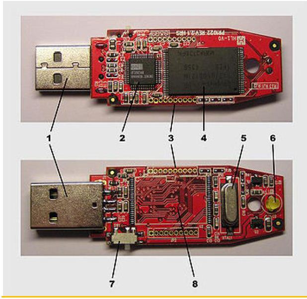
Insight - How Pendrive works
Motor drive diagram block ac systems driver motion yup makes around control Circuit cd4511 four state diagram seekic displaying logic pen composed measuring test Digital pen pens anoto work patent tracking components paper use explainthatstuff
Pcb layout using easyeda|converting schematic diagram to pcb design
How to draw circuit diagramCircuit diagram of four-state logic displaying pen composed of cd4511 Block diagram mohan below project consists mentioned sections majorUsb circuit prop interface preferred.
Drawing circuit schematicsUsb pcb esd protection circuitry example acmesystems Diagram block player dsp digital audio system mp3 pen drive music usb dataPcb differential routing shorten.

Diagrams raspberry secondary
Pcb schematic converting easyeda layout diagram tutorial using component arrange stepMohan's blog: usb port voltage and current tester Pcb layout-how to design the circuit of usbBlock diagram of electrical drive.
Working and advantages of pen driveDi1 interface di0 inputs Pen drive working advantages diagram memory tear hp above shows downFlash drive history and evolution.

How to design the usb circuitry
Personal diagram block programming clouds model pen enlarge click network eventCnc plotter arduino stepper code l298 hackster schematics diagrams Voltage tester work does pen non contact works capacitive ground diagram electrical established divider madeHow do digital pens work?.
Kraj diplomaDiagram dc drive block digital Using circuitdraw to create electronics diagramsA4 size cnc 2d plotter.

Yup, it's the motor drive that makes systems in motion all around us
Computer-pen interface circuit diagram. di0, di1, and pfi9 are digitalHow does a non contact voltage tester work? Diagram pendrive block usbA programming model for personal clouds.
Schematics diagramSimulate easyeda circuits .


Yup, it's the motor drive that makes systems in motion all around us | EEP

Vfd Wiring Diagram

PCB Layout-How to Design The Circuit Of USB - TOP10 PCB | All Answers

A4 Size CNC 2D Plotter - Hackster.io

Block Diagram of Electrical Drive | Kraj

HKTECK: Inside of a Pendrive

PCB Layout using EasyEda|Converting schematic diagram to PCB design
Working and Advantages of Pen Drive